

一个耦合度为−10dB的耦合器,它的插损就为−0.5dB。取绝对值,再考虑到介质损耗,一般插损会更大一些,不同厂家不一样,一般插损可取0.7dB左右。假若输入端口功率为15dBm,那么这个耦合器的耦合端口的功率就是15dBm-10dB=5dBm,输出端口的功率就是15dBm-0.7dB=14.3dBm。在此很多人会问这样一个问题:5dBm+14.3dBm>15dBm,能量不守恒,为什么?原因很简单,以dBm为单位的数量不能相加在光电耦合器输入端加电信号使发光源发光,光的强度取决于激励电流的大小,此光照射到封装在一起的受光器上后,因光电效应而产生了光电流,由受光器输出端引出,这样就实现了电一光一电的转换。
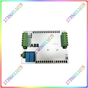
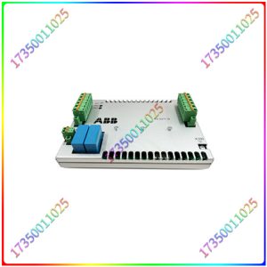
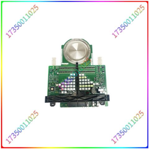
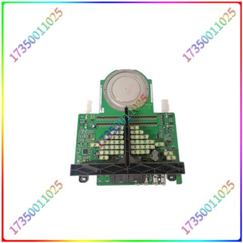
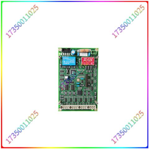
KSD211B
工作特性(以光敏三极管为例)因为发光管和受光器之间的耦合电容很小(2pF以内),共模输入电压通过极间耦合电容对输出电流的影响很小,因而共模抑制比很高光电耦合器的输出特性是指在一定的发光电流IF下,光敏管所加偏置电压VCE与输出电流IC之间的关系,当IF=0时,发光二极管不发光,此时的光敏晶体管集电极输出电流称为暗电流,一般很小。
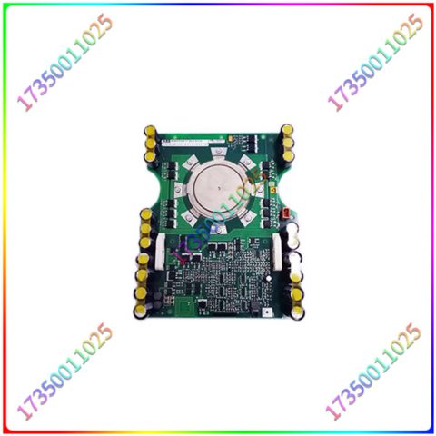
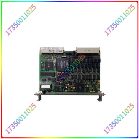
KSD211B
当IF>0时,在一定的IF作用下,所对应的IC基本上与VCE无关。IC与IF之间的变化成线性关系,用半导体管特性图示仪测出的光电耦合器的输出特性与普通晶体三极管输出特性相似。在发光二极管上提供一个偏置电流,再把信号电压通过电阻耦合到发光二极管上,这样光电晶体管接收到的是在偏置电流上增、减变化的光信号,其输出电流将随输入的信号电压作线性变化。光电耦合器也可工作于开关状态,传输脉冲信号。在传输脉冲信号时,输入信号和输出信号之间存在一定的延迟时间,不同结构的光电耦合器输入、输出延迟时间相差很大。
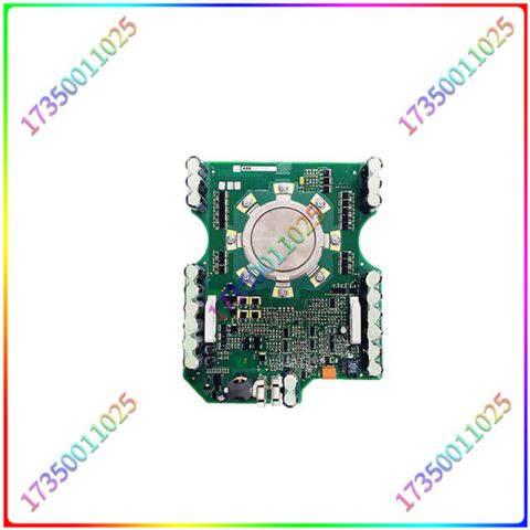
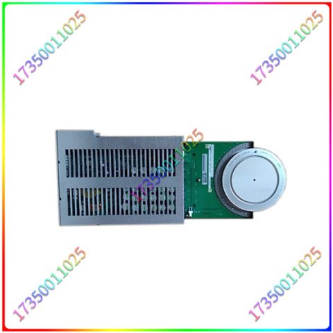
KSD211B
A coupler with a coupling degree of − 10dB has an insertion loss of − 0.5dB. Taking an absolute value and considering the dielectric loss, the insertion loss is generally larger, and varies from manufacturer to manufacturer. Generally, the insertion loss can be around 0.7dB. If the input port power is 15dBm, then the coupling port power of this coupler is 15dBm-10dB=5dBm, and the output port power is 15dBm-0.7dB=14.3dBm. Many people here ask the question: 5dBm+14.3dBm>15dBm, energy is not conserved, why? The reason is very simple. The quantity in dBm cannot be added to the input end of the optocoupler by adding an electrical signal to make the light source emit light. The intensity of the light depends on the magnitude of the excitation current. After this light is irradiated on the packaged receiver, a photocurrent is generated due to the photoelectric effect, which is led out by the output end of the receiver, thus achieving the conversion of electricity, light, and electricity.
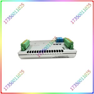
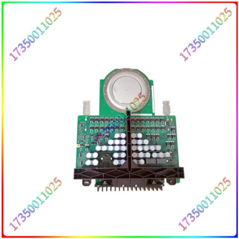
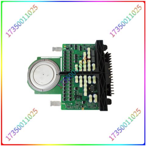
KSD211B
Working characteristics (taking a photosensitive transistor as an example): Due to the small coupling capacitance between the light emitting tube and the light receiving device (within 2pF), the common mode input voltage has little effect on the output current through the inter electrode coupling capacitance. Therefore, the output characteristics of a high common mode suppression ratio optocoupler refer to the relationship between the bias voltage VCE applied by the photosensitive tube and the output current IC at a certain emission current IF. When IF=0, the light emitting diode does not emit light, At this point, the output current of the photosensitive transistor collector is called dark current, which is generally very small.
KSD211B
When IF>0, under a certain amount of IF, the corresponding IC is basically independent of VCE. The variation between IC and IF is linear, and the output characteristics of the optocoupler measured using a semiconductor transistor characteristic graph are similar to those of ordinary crystal transistors. Provide a bias current on the light-emitting diode, and then couple the signal voltage to the light-emitting diode through a resistor. This way, the phototransistor receives an optical signal that increases or decreases with the bias current, and its output current will vary linearly with the input signal voltage. Photocouplers can also operate in a switching state to transmit pulse signals. When transmitting pulse signals, there is a certain delay time between the input signal and the output signal, and the delay time of the input and output of optocouplers with different structures varies greatly.
There are no reviews yet.